More efficient output of the assembly line with Keiron

Keiron’s LiFT printer enables a more controlled and repeatable paste printing process to improve the quality of the end-product and brings you a significant increase in uptime

Keiron’s LiFT technology delivers nano-precision printing, ensuring consistent dot sizes and placement accuracy with real-time quality control.

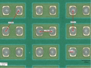
Our LiFT laser-guided solder paste deposition ensures the paste lands exactly where it's needed, with a dot that has a deviation of no more than 25%. This compared to an industry average of 75%
on reliability
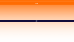
Less rework and fewer quality issues means higher production throughput. We see an average of a first pass yield of 60% with current industry standards vs 95% with Keiron
Keiron’s fully digital process optimizes efficiency, reducing changeover time, increasing Overall Equipment Effectiveness (OEE), and minimizing operator dependency.

Keiron's system enables faster program changes for NPIs and continuous operation. This compared to a an average 30 minute effort for screen- and jet printers
Higher automation and efficiency means fewer operators are needed.
Due to fewer manual activities.
Keiron’s LIFT technology eliminates the need for traditional consumables such as stencils, nozzles, and ejectors, transforming the SMT printing process into a fully digital, contactless solution which reduces costs and increases uptime.
on CAPEX

No stencils, no nozzles, no ejectors means nearly eliminating recurring material expenses.

In a high mix and low to medium volume environment removing stencil changes and nozzle maintenance allows for a fully digital, continuous production process.
Keiron’s integrated closed-loop inspection prevents defects before they occur, eliminating rework and manual inspection while ensuring consistent quality.
LiFT’s closed-loop SPM system prevents defects in real time, leading to fewer rework at the end of the line and a higher output.
LiFT technology guarantees perfect solder paste deposition with real-time closed-loop inspection, ensuring less defects, fewer rework, and maximum yield. 100% measured.
Achieve unmatched precision with Keiron’s LiFT technology. Prints ultra-small deposits (01005) with 100% precision, right next to ultra-large deposits from large components.
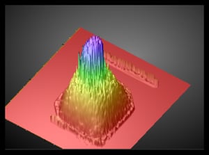
Verify true volume solder paste with Keiron’s integrated 3D Solder Paste Volume Metrology (SPVM)—eliminating the need for a separate SPI system by providing precise, real-time validation within the solder paste printing process.


VDL TBP Electronics
“We've been collaborating with Keiron for quite some time, and their innovative technology is delivering significant advantages—not just for us, but for the industry as a whole. The unique combination of flexibility and high-speed performance marks an important step toward the future of electronics—where we can truly print anything."
Capabilities and processing
Process window:
Min 01005 – 0.3 mm pitch components
Max: Ground plates of QFP256 components
Volume (acc. IPC–A–610 class 3):
Pad size >= 01005
Single dot repeatability:
±1nL or ±25% ±2σ, whichever is larger
Capabilities and processing
Process window:
Min 01005 – 0.3 mm pitch components
Max: Ground plates of QFP256 components
Volume (acc. IPC–A–610 class 3):
Pad size >= 01005
Single dot repeatability:
±1nL or ±25% ±2σ, whichever is larger
Performance metrics
Total cycle time
equal or faster with a pick and place machine of average 30,000 cph nett speed
SMEMA, CFX (roadmap)
AAR (stencil files), Gerber files (2025) and ODB++ (Coming Soon)
Performance metrics
Total cycle time
equal or faster with a pick and place machine of average 30,000 cph nett speed
SMEMA, CFX (roadmap)
AAR (stencil files), Gerber files (2025) and ODB++ (Coming Soon)
Board & Paste requirements
Board & Paste requirements
Board size:
≤580x508mm (20 in x 20.8 in.)
Thickness:
1-3mm, according PCB guideline
Positioning (within single PCB):
Absolute accuracy (X,Y): ±50 μm ±3σ
Solder paste:
Type 4 -6 leaded and lead-free or higher, (01005 Type 5/6)
Do you have questions? Talk with an expert